慶應義塾大学
2007年度 秋学期
コンピューター・アーキテクチャ
Computer Architecture
第5回 11月12日
Lecture 5, November 12: Memory: Caching and Memory Hierarchy
Outline of This Lecture
- Followup on Pipelining
- Review: Processor Performance Equation
- Principle of Caching
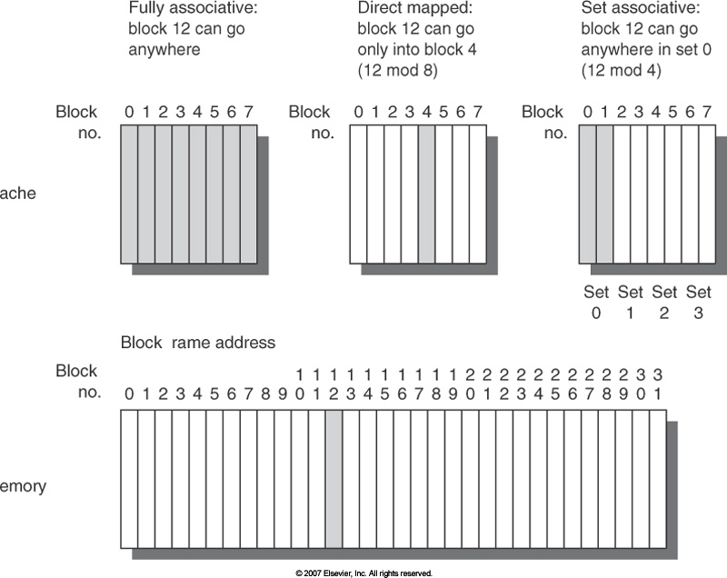
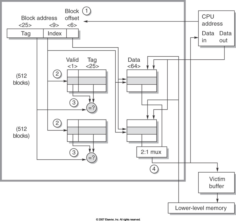
- Basic Fixed-Block Size Cache Organizations:
Four Questions
- Cache Performance
- Six Cache Optimizations
- Okay, Why?
- Final Thoughts: The Full Memory Hierarchy
- Homework
Followup on Pipelining
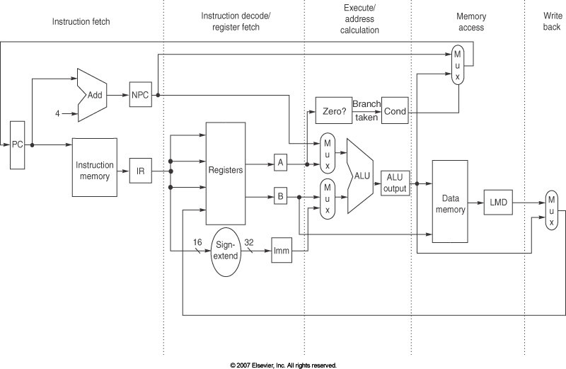
The five-stage pipeline we discussed last week is far from the only
way to divide the work in a pipeline. The Intel Prescott
microprocessor (which went into production in Feb. 2004) had
a thirty stage pipeline! Filling that pipeline takes some
serious time, so every branch is a problem.
The most famous pipeline of all:
I also did not explain the difference between
the rs, rt, and rd
register specifications in an instruction very well. The distinction
is architecture-specific, of course, and not the most important factor
in understanding instruction execution, but we should get it right.
Review: Processor Performance Equation
In the first lecture we saw the processor performance
equation:
CPU time = |
(seconds
)/
program
|
= |
(Instructions
)/
program
|
× |
(Clock cycles
)/
Instruction
|
× |
(Seconds
)/
Clock cycle
|
All three terms are actually interdependent. We know that the last
term in that equation is the inverse of clock speed, and that clock
speed goes up as you deepen the pipeline (assuming a good pipeline
design). The first term depends on the instruction set design; after
the last three lectures, you should have a better feel for what that
involves, but it will rarely vary by more than a factor of two or so
between architectures. The interesting term for this lecture is the
middle one: what is the average clock cycles per instruction,
or CPI?
Principle of Caching
Cache: a safe place for hiding or storing things.
Webster's New World Dictionary of the American Language, Second
College Edition (1976)
A cache, in computer terms, is usually a "nearby" place where a
copy of "far away" data is kept. This caching behavior is done
for a fundamental reason: performance. There are many common types of
caches:
- DNS (Internet name server) caches
- Web caches
- File system caches
- CPU caches
In this lecture, we are primarily concerned with the last of these.
This is the point where I admit that last week I told a white lie: in
the MEM stage of the pipeline, results came back from memory in
one clock cycle. In reality, they don't. We need to discuss cache
hits and cache misses, hit time and miss
penalty.
With those values, we can determine the actual average CPI and
expected execution time for a program.
Basic Fixed-Block Size Cache Organizations: Four Questions
Cache Performance
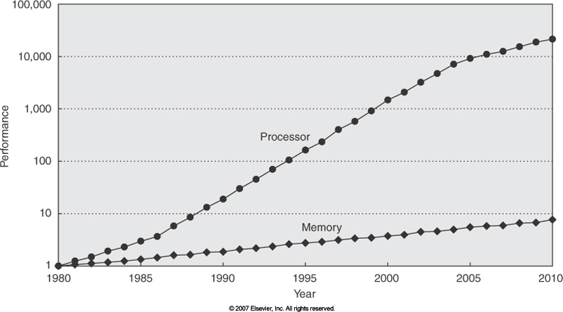
Above, we alluded to the change in system performance based on memory
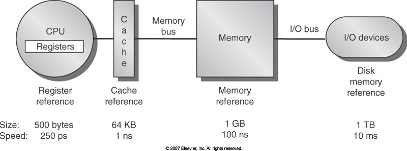
latency. The figure above and Fig. 5.28 in the text give a hint as to
the typical latencies of some important memories:
- Register: 250psec, 1 clock cycle
- L1 cache: 1nsec, 1 to 4 clock cycles
- L2 cache: a few nsec, 7-23 clock cycles
- Main memory: 30-50nsec, 50-100 clock cycles!
This list should make it extremely clear that a cache miss
results in a very large miss penalty. The average memory
access time then becomes:
Avg. memory access time | = |
Hit time + Miss rate × Miss penalty
|
Let's review the MIPS pipeline that we saw last week:
In our simple model of its performance, we assumed memory could be
accessed in one clock cycle, but obviously that's not true. If the
pipeline stalls here waiting on main memory, worst case, performance
could drop by a factor of one hundred!
Fortunately, many processors support out of order execution,
which allows other instructions to complete while a load is waiting on
memory, provided that there is no data hazard.
It's obvious from that high miss penalty that cache hit rates must
exceed 90%, indeed, usually are above 95%. Even a small improvement
in cache hit rate can make a large improvement in system
performance.
Six Basic Optimizations
- Larger block size to reduce miss rate
- Larger caches to reduce miss rate
- Higher associativity to reduce miss rate
- Multilevel caches to reduce miss penalty
- Giving priority to read misses over writes to reduce miss
penalty
- Avoiding address translation during indexing of the cache to
reduce hit time
Okay, Why?
So far, we have taken it as more or less given that caches are
desirable. But what are the technological factors that force us to
use multiple levels of memory? Why not just use the fastest type for
all memory?
The principle reason is that there is a direct tradeoff between size
and performance: it's always easier to look through a small number of
things than a large number of things when you're looking for
something. In computer chips, it's also not possible to fit all of
the RAM we would like to have into the same chip with the CPU, in
general-purpose systems; you likely have a couple of dozen memory
chips in your laptop.
In standard computer technology, too, we have the distinction
of DRAM versus SRAM. DRAM is slower, but much denser,
and is therefore much cheaper. SRAM is faster and more expensive.
SRAM is generally used for on-chip caches. The capacity of DRAM is
roughly 4-8 times that of SRAM, while SRAM is 8-16 times faster and
8-16 times more expensive.
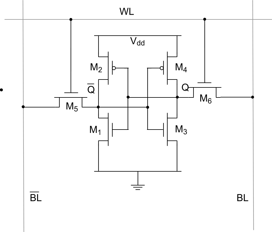
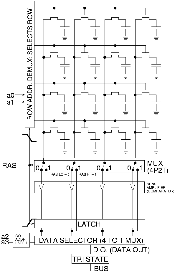
An SRAM cell typically requires six transistors, while a DRAM cell
requires only one. DRAMs are often read in bursts that fill
at least one cache block.
Final Thoughts: The Full Memory Hierarchy
We have talked about "main memory" and "cache memory", but in reality
memory is a hierarchy with a number of levels:
- Registers
- L1 (on-chip) cache
- L2 (on-chip) cache
- L3 (off-chip) cache
- Main memory
- Hard disk
- Tape
Ideally one would desire an indefinitely large memory capacity such
that any particular...word would be immediately available...We
are...forced to recognize the possibility of constructing a hierarchy
of memories, each of which has geater capacity than the preceding but
which is less quickly accessible.
A.W. Burks, H.H. Goldstine, and J. von Neumann,
Preliminary Discussion of the Logical Design of an Electronic
Computing Instrument (1946)
宿題
Homework
This week's homework (submit via email):
- Clearly we need more practice with hexadecimal notation and bit
fields. Assuming the above example of the AMD Opteron processor,
with 40-bit physical addresses, identify
the tag, index, and block offset of the
following addresses:
- 0x1000
- 0x1004
- 0x1044
- 0x1049
- 0x81231000
- 0xA1239004
- 0xA1239913
- Assume a system with a 1GHz system clock, only one level of cache,
and that L1 access is 1 clock cycle and main memory is 50 clock cycles.
- Plot the average memory access time as a function of
hit rate.
- Plot the expected completion time for one billion instructions
as a function of cache hit rate.
Next Lecture
Next week, we will continue with the discussion of cache behavior,
then shift into virtual memory.
Next lecture:
第6回 11月19日
Lecture 6, November 19: Memory: Virtual Memory
Readings for next time:
- Follow-up from this lecture: Appendix C.1, C.2 and C.3, Section 5.3
- For next time: Section 5.4
Additional Information
その他