慶應義塾大学
2008年度 秋学期
コンピューター・アーキテクチャ
Computer Architecture
第8回 11月18日
Lecture 8, November 18: Memory: Caching and Memory Hierarchy, Virtual Memory
Outline of This Lecture
- Review: Basic Fixed-Block Size Cache Organizations:
Four Questions
- Cache Performance
- Six Cache Optimizations
- Okay, Why?
- The Full Memory Hierarchy
- Virtual Memory
- Homework
Review: Basic Fixed-Block Size Cache Organizations: Four Questions
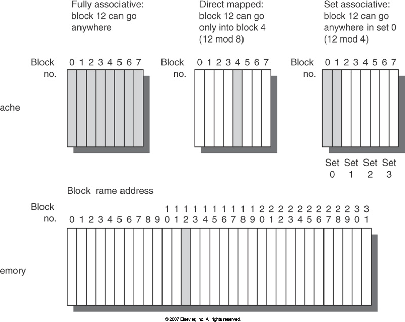
- Where can a block be placed in the upper level?
In hardware, caches are usually organized as direct
mapped, set associative, or fully associative.
- How is a block found if it is in the upper level?
Generally, an address is divided into the block address and
the block offset. The block address is further divided into
the tag and the index.
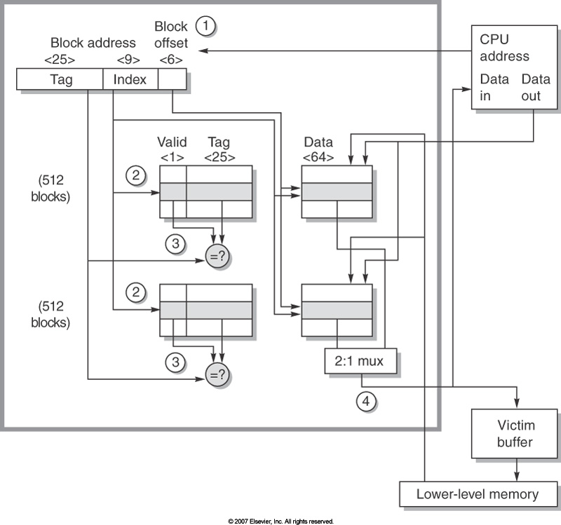
The AMD Opteron processor uses a 64KB cache, two-way set
associative, 64 byte blocks. Addresses are 40 bit physical addresses.
In the figure below, you can see the physical address in the upper
left hand corner.
- The upper (high-order, or left-most) 25 bits of
the address are the tag,
- the next (middle) 9 bits are the index, and
- the low-order 6 bits are the block offset.
- Which block should be replaced on a miss?
- Random
- Least-recently used (LRU)
- First in, first out (FIFO)
- What happens on a write?
- Write through
- Write back
- Write allocate or no-write allocate?
Cache Performance
Above, we alluded to the change in system performance based on memory
latency. The figure above and Fig. 5.28 in the text give a hint as to
the typical latencies of some important memories:
- Register: 250psec, 1 clock cycle
- L1 cache: 1nsec, 1 to 4 clock cycles
- L2 cache: a few nsec, 7-23 clock cycles
- Main memory: 30-50nsec, 50-100 clock cycles!
This list should make it extremely clear that a cache miss
results in a very large miss penalty. The average memory
access time then becomes:
Avg. memory access time | = |
Hit time + Miss rate × Miss penalty
|
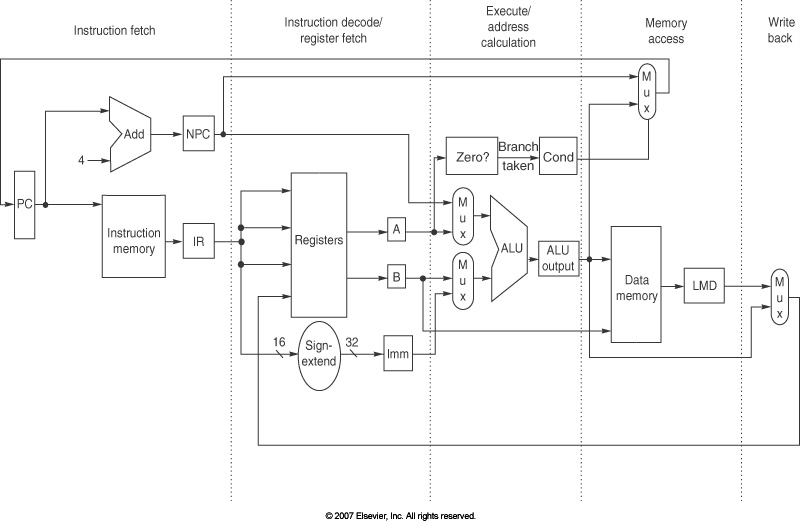
Let's review the MIPS pipeline that we saw last week:
In our simple model of its performance, we assumed memory could be
accessed in one clock cycle, but obviously that's not true. If the
pipeline stalls here waiting on main memory, worst case, performance
could drop by a factor of one hundred!
Fortunately, many processors support out of order execution,
which allows other instructions to complete while a load is waiting on
memory, provided that there is no data hazard.
It's obvious from that high miss penalty that cache hit rates must
exceed 90%, indeed, usually are above 95%. Even a small improvement
in cache hit rate can make a large improvement in system
performance.
Six Basic Optimizations
- Larger block size to reduce miss rate
- Larger caches to reduce miss rate
- Higher associativity to reduce miss rate
- Multilevel caches to reduce miss penalty
- Giving priority to read misses over writes to reduce miss
penalty
- Avoiding address translation during indexing of the cache to
reduce hit time
Okay, Why?
So far, we have taken it as more or less given that caches are
desirable. But what are the technological factors that force us to
use multiple levels of memory? Why not just use the fastest type for
all memory?
The principle reason is that there is a direct tradeoff between size
and performance: it's always easier to look through a small number of
things than a large number of things when you're looking for
something. In computer chips, it's also not possible to fit all of
the RAM we would like to have into the same chip with the CPU, in
general-purpose systems; you likely have a couple of dozen memory
chips in your laptop.
In standard computer technology, too, we have the distinction
of DRAM versus SRAM. DRAM is slower, but much denser,
and is therefore much cheaper. SRAM is faster and more expensive.
SRAM is generally used for on-chip caches. The capacity of DRAM is
roughly 4-8 times that of SRAM, while SRAM is 8-16 times faster and
8-16 times more expensive.
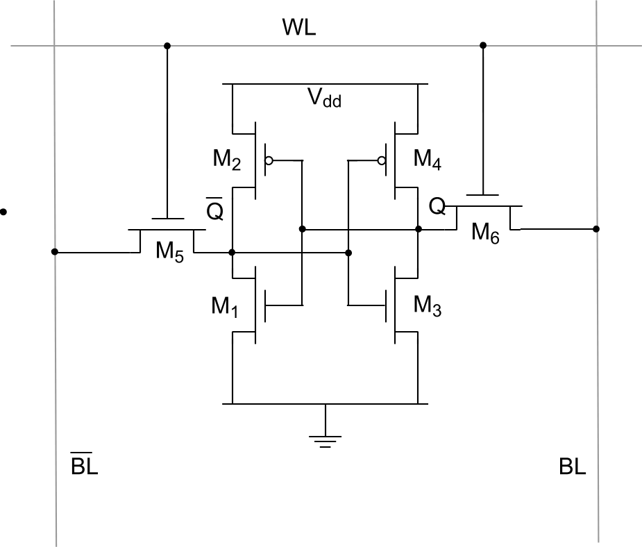
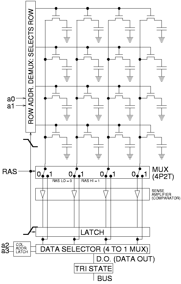
An SRAM cell typically requires six transistors, while a DRAM cell
requires only one. DRAMs are often read in bursts that fill
at least one cache block.
The Full Memory Hierarchy
We have talked about "main memory" and "cache memory", but in reality
memory is a hierarchy with a number of levels:
- Registers
- L1 (on-chip) cache
- L2 (on-chip) cache
- L3 (off-chip) cache
- Main memory
- Hard disk
- Tape
Ideally one would desire an indefinitely large memory capacity such
that any particular...word would be immediately available...We
are...forced to recognize the possibility of constructing a hierarchy
of memories, each of which has geater capacity than the preceding but
which is less quickly accessible.
A.W. Burks, H.H. Goldstine, and J. von Neumann,
Preliminary Discussion of the Logical Design of an Electronic
Computing Instrument (1946)
Virtual Memory
Memory Map
The most important concept tool for visualizing the location of data
is the memory map. Memory maps can be drawn with high
addresses at the top or the bottom.
(Image from NCSU.)
Introduction to Virtual Memory
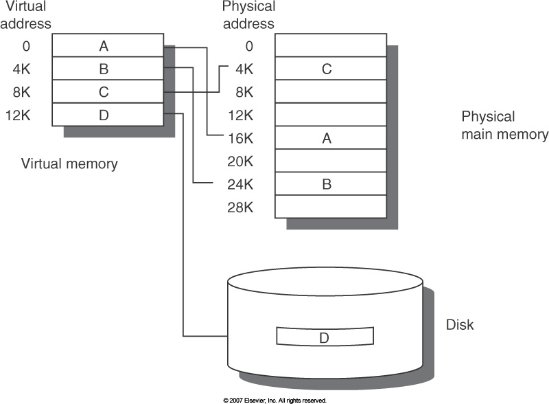
Finally, we come to virtual memory (仮想記録). With virtual
memory, each process has its own address space. This
concept is a very important instance of naming. Virtual memory
(VM) provides several important capabilities:
- VM hides some of the layers of the memory hierarchy.
- VM's most common use is to make memory appear larger than it is.
- VM also provides protection and naming, and those
are independent of the above role.
In most modern microprocessors intended for general-purpose use, a
memory management unit, or MMU, is built into the
hardware. The MMU's job is to translate virtual addresses into
physical addresses.
A basic example:
Whether Windows, MacOS, or some other Unix variant, a program
runs in a process, and each process has its own virtual
memory space.
Page Tables
Viritual memory is usually done by dividing memory up into
pages, which in Unix systems are typically, but not
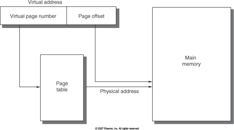
necessarily, four kilobytes (4KB) each. The page table is the
data structure that holds the mapping from virtual to physical
addresses. The page frame is the actual physical storage in
memory. The basic principle of a page table:
The simplest approach would be a large, flat page table with one entry
per page. The entries are known as page table entries, or
PTEs. However, this approach results in a page table that is
too large to fit inside the MMU itself, meaning that it has to be in
memory. In fact, for a 4GB address space, with 32-bit PTEs and 4KB
pages, the page table alone is 4MB! That's big when you consider that
there might be a hundred processes running on your system.
The solution is multi-level page tables. As the size of the
process grows, additional pages are allocated, and when they are
allocated the matching part of the page table is filled in.
The translation from virtual to physical address must be fast.
This fact argues for as much of the translation as possible to be done
in hardware, but the tradeoff is more complex hardware, and more
expensive process switches. Since it is not practical to put the
entire page table in the MMU, the MMU includes what is called the
TLB: translation lookaside buffer.
Linux Page Tables
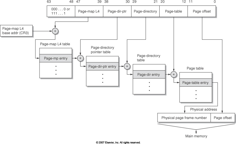
PGD is the page global directory, in Linux
terminology. PTE is page table entry, of course. PMD
is page middle directory. Note the similarity to the Opteron
diagram above, except that this figure shows only three levels, each
supporting 512 entries per page; a patch for 64-bit systems supports
the fourth level, known as the PML4 level. The
software-defined use of the page tables must correspond to the
hardware, and will be different on different processors, though the
principle is the same.
The hardware-defined page table entries and page directory entries in
a 32-bit Intel (IA-32) machine:
(Images from O'Reilly's book on Linux device drivers, and from
lvsp.org.)
Putting it All Together
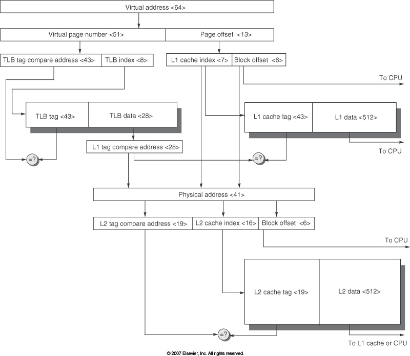
A hypothetical memory hierarchy, with 64-bit virtual addresses, 41-bit
physical addresses, and a two-level cache. Pages are 8KB. The TLB is
direct mapped, with 256 entries. The L1 cache is direct-mapped, 8KB,
and the L2 cache is direct-mapped 4MB. Both use 64-byte blocks.
宿題
Homework
This week's homework (submit via email):
- Write down the equation for calculating the average memory access
time for a two-level cache.
- Following the example from our lecture on pipelining, suggest a
modification to the five-stage pipeline to accommodate the memory
architecture above.
- How many stages must the pipeline have to
support the L1 cache?
- When data must be retrieved from L2 cache, how many cycles
will the processor stall?
- Using one of the examples from Fig. 5.28 from the text, how
many cycles will the processor stall to retrieve data from main
memory?
- Suggest an alternative to waiting for main memory. Can the
processor achieve useful work while waiting?
Next Lecture
No lecture next week! The following week is the first of two
lectures on multiprocessors.
Next lecture:
第9回 12月2日
Lecture 9, December 2: Systems: Shared-Memory Multiprocessors
- Follow-up from this lecture:
- H-P: Appendix C.4 and C.5, and Section 5.4
- For next time:
- Sections 4.1, 4.2, and 4.3
Additional Information
その他